Xiamen Tmax Battery Equipments Limited was set up as a manufacturer in 1995, dealing with Laboratory equipments, technology, etc. We have total manufacturing facilities of around 2, 000 square meters and more than 100 staff. Owning a group of experie-nced engineers and staffs, we can bring you not only reliable products and technology, but also excellent services and real value you will expect and enjoy.
Vacuum Sputtering Coater: Advanced Thin-Film Deposition Equipment for Precision Surface Engineering
Introduction
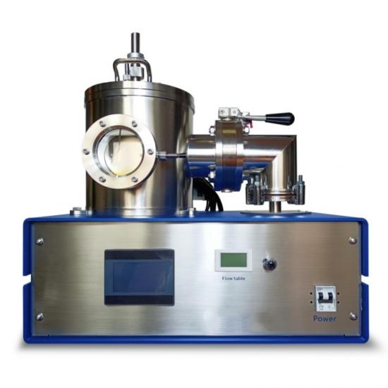
A Vacuum Sputtering Coater is an advanced physical vapor deposition (PVD) system used to deposit high-quality thin films onto a wide variety of substrates. By utilizing plasma-assisted sputtering under high-vacuum conditions, this equipment enables the formation of dense, uniform, and highly adherent coatings with exceptional precision. Vacuum sputtering technology has become an indispensable process in industries such as semiconductors, electronics, optics, aerospace, automotive manufacturing, medical devices, and advanced materials research.
Compared with conventional coating methods, a Vacuum Sputtering Coater provides superior film uniformity, excellent material utilization, and precise control over coating thickness and composition. As modern manufacturing demands increasingly sophisticated functional coatings, vacuum sputtering systems continue to evolve with higher automation, improved deposition efficiency, and intelligent process control.
---
What Is a Vacuum Sputtering Coater?
A Vacuum Sputtering Coater is a sophisticated PVD machine that deposits thin films by ejecting atoms from a solid target material through ion bombardment within a vacuum chamber. During the sputtering process, inert gas—typically argon—is introduced into the chamber and ionized to generate plasma. Positively charged argon ions accelerate toward the negatively charged target, dislodging atoms that travel through the vacuum and condense onto the substrate surface to form a thin, uniform coating.
A typical Vacuum Sputtering Coater consists of the following components:
* High-vacuum chamber
* Magnetron sputtering cathodes
* Target materials
* Vacuum pumping system
* Gas flow control system
* Plasma power supply (DC, RF, or pulsed DC)
* Substrate holder and rotation system
* Thickness monitoring system
* Temperature control system
* Programmable control software
Modern systems can be configured for single-target, multi-target, or co-sputtering applications to produce complex multilayer or composite thin films.
---
Key Features
Modern Vacuum Sputtering Coaters incorporate numerous advanced features that ensure high-quality film deposition and efficient operation.
High Vacuum Environment
The deposition chamber typically operates at pressures between 10⁻⁶ and 10⁻⁸ Torr, minimizing contamination from oxygen, moisture, and airborne particles. This clean environment is essential for producing high-purity thin films with excellent performance.
Excellent Film Uniformity
Magnetron sputtering technology provides highly uniform coating thickness across substrates of various sizes. Rotating substrate holders and optimized target arrangements further improve deposition consistency.
Wide Material Compatibility
Vacuum sputtering systems can deposit a broad range of materials, including:
* Gold (Au)
* Silver (Ag)
* Aluminum (Al)
* Copper (Cu)
* Titanium (Ti)
* Chromium (Cr)
* Nickel (Ni)
* Platinum (Pt)
* Silicon (Si)
* Indium Tin Oxide (ITO)
* Titanium Nitride (TiN)
* Aluminum Oxide (Al₂O₃)
This versatility makes the equipment suitable for numerous industrial applications.
Precise Thickness Control
Integrated quartz crystal monitors and advanced process controllers allow operators to achieve nanometer-level thickness accuracy, ensuring consistent product quality.
Flexible Deposition Modes
Many systems support DC sputtering, RF sputtering, reactive sputtering, magnetron sputtering, and co-sputtering, enabling the deposition of metals, semiconductors, ceramics, and dielectric materials.
---
Vacuum Sputtering Process
The coating process follows several carefully controlled stages to ensure high-quality thin-film formation.
1. Substrate Preparation
The substrate is cleaned to remove contaminants such as dust, oils, and oxidation layers. Proper cleaning significantly improves film adhesion and coating quality.
2. Chamber Evacuation
The vacuum pumping system evacuates the chamber to achieve high-vacuum conditions, minimizing contamination during deposition.
3. Gas Introduction
High-purity argon gas is introduced into the chamber at a precisely controlled flow rate to establish the desired operating pressure.
4. Plasma Generation
A high-voltage power supply ionizes the argon gas, generating plasma. The positively charged ions accelerate toward the target material.
5. Target Sputtering
Ion bombardment ejects atoms from the target surface. These sputtered atoms travel through the vacuum chamber and deposit onto the substrate.
6. Thin Film Growth
The deposited atoms gradually form a dense, uniform thin film with controlled thickness, composition, and microstructure.
7. Cooling and Inspection
After deposition, the coated substrates cool before undergoing quality inspection for thickness, adhesion, surface morphology, and electrical or optical performance.
DC Sputtering Machines
Major Applications
Vacuum Sputtering Coaters are widely used in numerous high-technology industries.
Semiconductor Manufacturing
Integrated circuits, microprocessors, sensors, and semiconductor devices require sputtered thin films for conductive layers, barrier layers, and interconnections.
Optical Coatings
Vacuum sputtering is widely employed to manufacture anti-reflection coatings, mirrors, optical filters, beam splitters, and infrared coatings with excellent optical performance.
Display Technology
LCD, OLED, and touch panel manufacturing utilize sputtering systems to deposit transparent conductive oxides such as ITO and other functional layers.
Solar Cell Production
Thin-film photovoltaic devices rely on sputtered conductive, buffer, and protective layers to improve energy conversion efficiency.
Decorative Coatings
Titanium nitride, chromium nitride, and other decorative coatings provide attractive finishes with enhanced hardness and wear resistance for watches, jewelry, consumer electronics, and architectural hardware.
Medical Devices
Vacuum sputtering produces biocompatible coatings on surgical instruments, orthopedic implants, dental components, and medical sensors to improve corrosion resistance and durability.
Research and Development
Universities and research laboratories use Vacuum Sputtering Coaters for nanotechnology, advanced materials science, thin-film electronics, superconductors, and quantum device research.
---
Advantages of a Vacuum Sputtering Coater
Compared with many alternative coating technologies, a Vacuum Sputtering Coater offers numerous significant advantages.
Superior Film Adhesion
Sputtered atoms possess relatively high kinetic energy, producing dense films with excellent adhesion to the substrate.
High Film Density
The deposited coatings exhibit low porosity, improving mechanical strength, corrosion resistance, and long-term stability.
Excellent Thickness Uniformity
Carefully controlled plasma conditions and substrate movement ensure highly uniform coatings across large surface areas.
Broad Material Selection
The equipment can deposit conductive, insulating, magnetic, optical, and ceramic materials using various sputtering techniques.
Environmentally Friendly Process
Unlike some chemical coating methods, sputtering generally requires fewer hazardous chemicals and produces less waste.
High Process Repeatability
Computer-controlled process parameters ensure consistent coating quality across multiple production batches, making the technology ideal for industrial manufacturing.
---
Future Development Trends
As advanced manufacturing continues to evolve, Vacuum Sputtering Coaters are becoming increasingly intelligent, efficient, and versatile. Artificial intelligence and machine learning are being integrated into process control systems to optimize plasma stability, deposition rates, and coating quality in real time. Automated target exchange, predictive maintenance, and digital production monitoring are also enhancing operational efficiency.
Emerging technologies such as high-power impulse magnetron sputtering (HiPIMS), roll-to-roll sputtering, large-area coating systems, and hybrid deposition processes are expanding the capabilities of vacuum sputtering. These innovations are supporting next-generation applications in flexible electronics, solid-state batteries, semiconductor packaging, quantum computing, and advanced optical devices.
---
Conclusion
A Vacuum Sputtering Coater is a highly sophisticated thin-film deposition system that combines vacuum technology, plasma physics, and precision engineering to produce high-performance coatings for a wide range of industrial and scientific applications. Through controlled sputtering processes, it delivers dense, uniform, and highly adherent thin films with exceptional accuracy and repeatability.
With advantages including superior coating quality, broad material compatibility, precise thickness control, and excellent process stability, Vacuum Sputtering Coaters have become indispensable equipment in semiconductor manufacturing, optics, renewable energy, medical technology, and advanced research. As demand for functional thin films continues to grow, vacuum sputtering technology will remain at the forefront of modern surface engineering and next-generation manufacturing.