Xiamen Tmax Battery Equipments Limited was set up as a manufacturer in 1995, dealing with Laboratory equipments, technology, etc. We have total manufacturing facilities of around 2, 000 square meters and more than 100 staff. Owning a group of experie-nced engineers and staffs, we can bring you not only reliable products and technology, but also excellent services and real value you will expect and enjoy.
Sputtering Coater: Advanced Thin-Film Deposition Equipment for Precision Surface Engineering
Overview
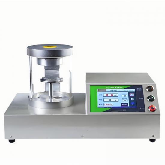
A Sputtering Coater is a high-performance vacuum deposition system used to produce thin films with exceptional uniformity, adhesion, and precision. Based on the physical vapor deposition (PVD) process, a sputtering coater utilizes plasma-generated ions to bombard a target material, ejecting atoms that are subsequently deposited onto the surface of a substrate. This technology is widely employed in semiconductor manufacturing, nanotechnology, optics, advanced battery research, MEMS fabrication, biomedical engineering, and materials science.
Modern Sputtering Coater systems are designed to accommodate a wide range of coating materials, including pure metals, alloys, oxides, nitrides, carbides, and composite materials. By integrating high-vacuum technology, magnetron sputtering sources, programmable process control, substrate rotation, and real-time monitoring, these machines deliver highly reproducible coatings for both laboratory research and industrial-scale production.
As industries increasingly require thinner, more functional, and higher-quality surface coatings, sputtering coaters have become indispensable equipment for manufacturing advanced electronic devices, optical components, energy storage systems, and precision instruments.
---
Key Characteristics
A modern Sputtering Coater incorporates advanced engineering features that ensure stable operation and superior coating performance.
High-Precision Film Deposition
One of the defining characteristics of a sputtering coater is its ability to deposit films with nanometer-level thickness control. Precise adjustment of deposition parameters enables users to produce coatings with highly consistent thickness and excellent repeatability.
Excellent Coating Uniformity
Advanced magnetron configurations, optimized plasma distribution, and rotating substrate holders ensure uniform deposition across the entire substrate surface. Uniform coatings are essential for semiconductor devices, optical components, and precision sensors.
High Vacuum Environment
The deposition chamber operates under high or ultra-high vacuum conditions, minimizing contamination from air, moisture, and impurities. This environment improves film purity, density, and adhesion.
Multiple Deposition Technologies
Modern sputtering coaters support various deposition methods, including:
* DC Magnetron Sputtering
* RF Magnetron Sputtering
* Pulsed DC Sputtering
* Reactive Sputtering
* Co-Sputtering
* Multi-Layer Thin-Film Deposition
These technologies enable the deposition of both conductive and non-conductive materials with excellent flexibility.
Intelligent Automation
Integrated control systems automatically regulate vacuum pressure, sputtering power, gas flow rate, substrate temperature, deposition time, and film thickness. Programmable recipes simplify operation while improving process consistency.
Flexible System Configuration
Many sputtering coaters feature modular designs with multiple target positions, allowing users to switch materials quickly or perform sequential and co-deposition processes for complex multilayer coatings.
---
Working Process
The operation of a Sputtering Coater follows a carefully controlled sequence to produce high-quality thin films.
Substrate Preparation
Before coating, substrates are cleaned using ultrasonic cleaning, plasma cleaning, or chemical treatments to remove dust, oils, and surface contaminants that could affect film adhesion.
Vacuum Generation
The substrates and sputtering targets are placed inside the vacuum chamber. Mechanical pumps and turbomolecular pumps evacuate the chamber to achieve the required base pressure, often below 1 × 10⁻⁶ Torr.
Plasma Formation
An inert process gas, typically argon, is introduced into the chamber. Electrical power ionizes the argon atoms, generating a stable plasma around the target material.
Target Sputtering
Positively charged argon ions accelerate toward the negatively charged target. The energetic collisions eject atoms from the target surface through momentum transfer.
Thin-Film Deposition
The sputtered atoms travel through the vacuum chamber and condense onto the substrate, forming a dense and uniform thin film. Process parameters such as chamber pressure, gas composition, sputtering power, substrate temperature, and deposition duration are precisely controlled to achieve the desired film properties.
Post-Coating Treatment
Depending on the application, coated samples may undergo annealing, plasma treatment, or additional surface modification to improve crystallinity, adhesion, conductivity, or optical performance.
Quality Inspection
After deposition, films are characterized using analytical techniques such as thickness measurement, surface roughness analysis, adhesion testing, electrical conductivity evaluation, optical transmission measurement, and microscopic inspection.
DC Sputtering Coater
Applications
The versatility of a Sputtering Coater enables its use across numerous high-technology industries.
Semiconductor Manufacturing
Sputtering coaters are widely used to deposit:
* Metal interconnects
* Barrier layers
* Contact electrodes
* Seed layers
* Gate materials
* Packaging films
These coatings are essential for integrated circuits and advanced semiconductor devices.
Optics and Photonics
The equipment is used to manufacture:
* Anti-reflective coatings
* Optical filters
* Dielectric mirrors
* Transparent conductive coatings
* Laser optics
* Infrared coatings
Battery and Energy Storage Research
Researchers employ sputtering coaters to fabricate:
* Thin-film lithium batteries
* Solid-state electrolytes
* Protective electrode coatings
* Current collectors
* Interface engineering layers
These coatings contribute to improved battery performance, stability, and cycle life.
MEMS and Microelectronics
Microelectromechanical devices rely on sputtered thin films for sensors, actuators, resonators, and integrated microsystems requiring precise electrical and mechanical properties.
Biomedical Engineering
Biocompatible thin films deposited by sputtering are used on surgical instruments, orthopedic implants, dental devices, and medical sensors to enhance wear resistance, corrosion resistance, and biological compatibility.
Advanced Materials Research
Universities and research institutes use sputtering coaters to investigate nanomaterials, superconductors, magnetic materials, catalysts, two-dimensional materials, and multifunctional thin-film systems.
---
Advantages
A Sputtering Coater offers numerous advantages over conventional coating technologies.
* Exceptional Film Quality: Produces dense, uniform, and highly adherent coatings with precise thickness control.
* Wide Material Compatibility: Supports deposition of metals, ceramics, alloys, oxides, nitrides, carbides, and composite materials.
* Low Contamination: High-vacuum operation minimizes impurities, ensuring high-purity films suitable for demanding scientific and industrial applications.
* Excellent Process Repeatability: Automated parameter control and programmable process recipes deliver highly reproducible results.
* Scalable Production: Suitable for laboratory research, pilot-scale development, and large-scale industrial manufacturing.
* Efficient Material Utilization: Magnetron sputtering technology improves target utilization, reducing material waste and operating costs.
* Versatile Coating Capability: Multi-target configurations and reactive sputtering processes enable the fabrication of complex multilayer and functional thin-film structures.
---
Conclusion
The Sputtering Coater is one of the most important thin-film deposition systems in modern manufacturing and scientific research. By combining high-vacuum technology, plasma physics, precision engineering, and intelligent automation, it enables the production of high-quality coatings with outstanding uniformity, purity, and performance.
From semiconductor fabrication and optical component manufacturing to battery development, biomedical devices, and advanced materials research, sputtering coaters continue to drive innovation across a wide range of industries. As demand grows for smaller electronic devices, more efficient energy storage systems, and advanced functional materials, the capabilities of sputtering coating technology will continue to expand. With ongoing improvements in magnetron design, process control, vacuum engineering, and multi-material deposition, the Sputtering Coater will remain an essential piece of equipment for laboratories, research institutions, and manufacturers seeking reliable, high-precision, and cost-effective thin-film deposition solutions.